Description
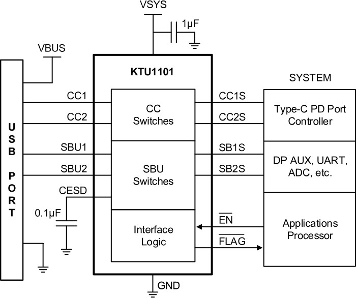
The KTU1101 provides ESD, surge, and overvoltage protection (OVP) for USB Type-C ports CC and SBU signal pins. ESD protection meets IEC61000-4-2 standards, eliminating the need for external TVS diodes. Surge protection meets IEC61000-4-5 standards, increasing immunity from power surges such as lightning strikes on the power lines while the USB cable is connected. Overvoltage protection (OVP) eliminates system damage due to physical or moisture-related shorts between the signal pins and VBUS at elevated PD voltage levels.
The SBU switches have low on-capacitance for passing high-speed signals. The CC1/2 switches have low onresistance for passing VCONN power up to 1.25A for CC power delivery communications. During dead battery conditions, internal 5.1kΩ resistors automatically pull down on CC1/2 to ensure that the up-stream source provides 5V to VBUS.
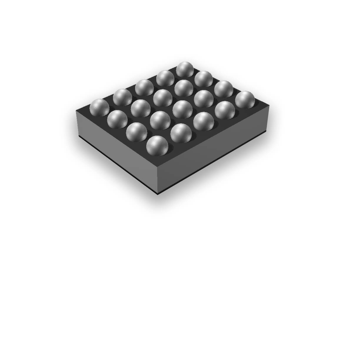
The KTU1101 is packaged in RoHS and Green compliant 2.060mm x 1.720mm wafer-level chip-scale package (WLCSP).


Features
- Overvoltage Protection (OVP)
- 24VDC Tolerance on CC1/2, SBU1/2
- Robust 27V overshoot clamping
- CC1/2 OVP = 5.8V typ
- SBU1/2 OVP = 4.8V typ
- Ultra-Fast 15ns Response Time
- IEC61000-4-5 Surge Protection
- ±80V Surge Tolerance on CC1/2
- ±35V Surge Tolerance on SBU1/2
- IEC61000-4-2 ESD Protection
- ±15kV air gap on CC1/2, SBU1/2
- ±8kV contact on CC1/2, SBU1/2
- ±2kV HBM on all pins (JEDEC JS-001-2017)
- Moisture Detection Compatible
- Over 10MΩ to ground on CC1/2, SBU1/2
- CC Switches
- 1.25A, 330mΩ
- Automatic 5.1kΩ dead battery pull-down
- SBU Switches
- 4Ω
- Reverse current blocking when disabled
- 2.5V to 5.5V Operating Supply Voltage Range
- -40°C to 85°C Operating Temperature Range
- Pb-free 20 bump WLCSP (0.4mm pitch)
Applications
- Smartphones
- Tablets
- Notebooks
- Monitors
- TVs
- Accessories
- AI/BT Loudspeakers
- IoT
- Any USB type-C port
| Package |
Dimensions |
Bumps |
Package Code |
| WLCSP54-20 |
2.050mm x 1.710mm x 0.620mm |
20 |
VF |
Parameters
| Vin (min) |
Vin (max) |
ON Resistance (Ω) |
OVP Trip Point (V) |
OVP Turn Off Response Time (ns) |
| 2.5V |
5.5V |
4/0.33Ω |
4.8/5.8 |
15ns |
Technical Documentation
Purchase
| Part Number |
Marking1 |
Operating Temperature |
Package |
| KTU1101EVF-TR |
MCXXYYZZZZ |
-40°C to +85°C |
WLCSP45-20 |


