Surge Protected, Single Input, Dual Output Load Switch with OVP
Description
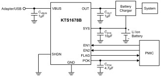
The KTS1678B features two low resistance power switches configured as single input, dual output, changeover switch. The input to both switches is protected against VBUS surge voltages of up to ±100V, and is also protected against over-voltage, with preset trip points on both the VBUS to OUT and VBUS to SYS paths, providing protection to downstream components from abnormal input conditions.
The main switch (VBUS to OUT) features a unidirectional active-LOW enabled 3.5A rated MOSFET, with an OVP trip point of 13.9V ±400mV. The secondary switch (VBUS to SYS) is an active-HIGH enabled, reverse-blocking 6.0A rated MOSFET, with an OVP trip point of 5.25V ±250mV. The input to both switches is rated up to a maximum of 28V.
When VBUS is greater than 2.7V, the POK LDO provides an “always ON” power source, regardless of the OVLO, EN1 ̅̅̅̅̅̅ and EN2 state, to power downstream components permitting operation without an installed battery.
The KTS1678B also features an active-HIGH SHUTDOWN pin to conserve power, plus over-temperature thermal protection.
The KTS1678B is packaged in advanced, fully “green” compliant, 2.96mm x 1.67mm, Wafer-Level Chip-Scale Package (WLCSP).
Features
- Single Input, Dual Output Low On- Resistance Switch
- VBUS to OUT: typ. 23mΩ
- VBUS to SYS: typ. 30mΩ (Reverse Blocking)
- Wide Input Voltage Range: 2.7V – 13.5V
- VBUS Abs Max: 28V
- Surge and ESD Protected Input
- Surge Protection
- IEC61000-4-5: > ±100V
-
- ESD Protection
- IEC61000-4-2 (Level 4) VBUS
- Contact: ±8kV
- Air Gap: ±15kV
- IEC61000-4-2 (Level 4) VBUS
-
- HBM: 2kV All Pins
- Integrated Overvoltage Protection (OVP)
- VBUS to OUT: 13.9V ±400mV
- VBUS to SYS: 5.25V ±250mV
- Maximum Continuous Current
- VBUS to OUT: 3.5A
- VBUS to SYS: 6A
- Dual Enable Control with Independent Shutdown Control
- Active LOW VBUS to OUT
- Active HIGH VBUS to SYS
- Active HIGH Shutdown
- VBUS detection LDO
- VBUS to SYS FLAG
- Over Temperature Protection
- Pb-free 28-Bump, WLCSP 2.96mm x 1.67mm
- -40°C to 85°C Operating Temperature Range
- ESD Protection
- Surge Protection
Applications
- Smartphones and Tablets
- Mobile Internet Devices
- Wearables
- Portable Devices
Packaging Information
| Package | Dimensions | Bumps | Package Code |
| WLCSP47-28 | 2.96mm x 1.67mm x 0.620mm | 28 | UQ |
Parameters
| Vin (min) | Vin (max) | ON Resistance | Max Current (A) | OVP Trip Point | Package |
| 2.7V | 13.5V | 23/30mΩ | 3.3/5.0A | VBUS-OUT: 13.9V VBUS-SYS: 5.25V |
WLCSP47-28 |
Technical Documentation
| Description | Documents | Type |
|---|---|---|
| Datasheet | KTS1678B-04d | |
| Package Outline Drawing | WLCSP47-28 UQ POD |
Purchase
| Part Number | Marking | Operating Temperature | Package |
| KTS1678BEUQ-TR | LTXXYYZZZZ | -40°C to +85°C | WLCSP-28 |
| Purchase Options |
|---|
| Buy from Digi-Key |
| Buy from Mouser |