3.0MHz High Efficiency Low IQ Synchronous Boost
Description
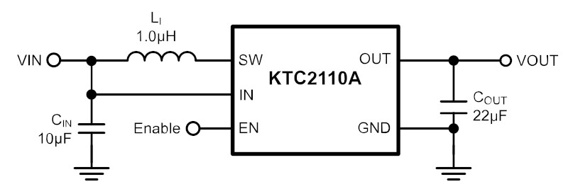
The KTC2110A features a high-efficiency, micropower synchronous boost for Lithium-Ion/Polymer battery applications.
The KTC2110A achieves high efficiency over a wide output current range by operating in auto PWM/PFM control. The control method is automatically selected according to the output load conditions.
The KTC2110A also features Bypass Mode which allows passing input power directly to output with over-current protection when the EN pin is pulled LOW.
The constant on-time design does not require any external compensation components, simplifying the design and also provides ultra-fast transient response.
Inrush current-limiting feature is provided to reduce inrush current, which minimizes the voltage droop on the battery when the device is turned on.
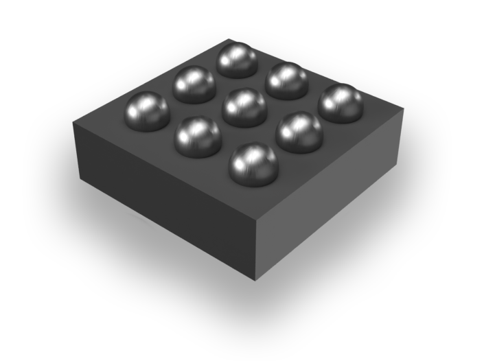
The KTC2110A is packaged in advanced, RoHS and Green compliant, 1.38mm x 1.38mm, 9-balls Wafer-Level Chip-Scale Package (WLCSP).
Features
- Wide Input Voltage Range: 2.5V to 5.5V
- Output Voltage 5.4V
- IOUT up to 1.0 A at VOUT = 5.4 V, VIN ≥ 3.0 V
- 3MHz PWM Switching Frequency
- High Efficiency and Low Quiescent Current
- Over 95% Efficiency
- 35μA Quiescent Current in Bypass Mode
- 55μA Quiescent Current in PFM Operation
- ±2% DC Voltage Accuracy in PWM mode
- Undervoltage Lockout (UVLO)
- Short Circuit Protection
- Hiccup Current Limit
- Over Temperature Protection
- Output Capacitor Pre-Charge and Soft-Start
- Pb-free 9-Bump, WLCSP 1.38mm x 1.38mm
- RoHS and Green Compliant
- -40°C to 85°C Operating Temperature Range
Applications
- Smartphones and Tablets
- Mobile Internet Devices
- USB OTG
- Wearables
- NFC Applications
- Portable Devices
Packaging Information
| Package | Dimensions | Bumps | Package Code |
| WLCSP33-9 | 1.38mm x 1.38mm x 0.62mm | 9 | CAA |
Parameters
| Vin (min) | Vin (max) | Vout | Iout | IQ | Control | FSW |
| 2.5V | 5.5V | 5.4V | 1.0A | 55µA | EN | 3.0MHz |
Technical Documentation
| Description | Documents | Type |
|---|---|---|
| Datasheet | KTC2110A-04a | |
| Package Outline Drawing | WLCSP33-9 CAA POD |
Purchase
| Part Number | Marking | Operating Temperature | Package |
| KTC2110AECAA-D-TR | NWXXYYZZZZ | -40°C to +85°C | WLCSP33-9 |
| Purchase Options |
|---|
| Buy from Digi-Key |
| Buy from Mouser |