Description
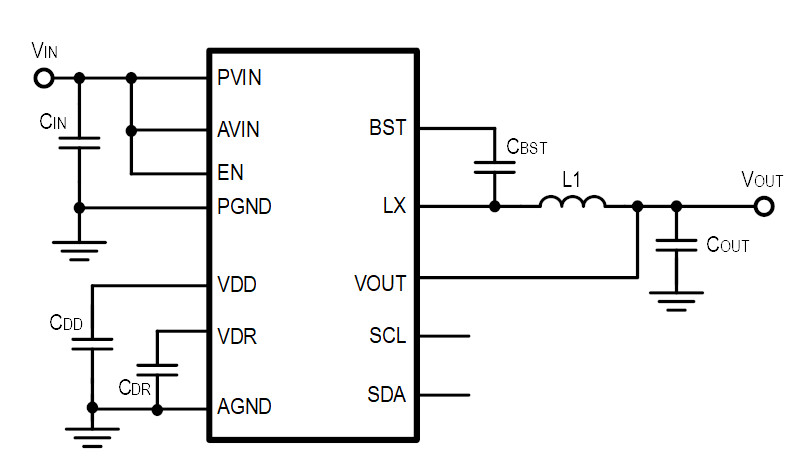
The KTB8371 is 5A, 17V synchronous buck regulators with integrated high-side and low-side power FETs. The device operates over a wide input voltage range to support a variety of applications with input voltage from regulated 5V and 12V power rails and multicell batteries.
KTB8371 employs Kinetic’s proprietary advanced adaptive on-time (AOT) control for fast transient response and high output voltage accuracy. This control technique eliminates the external loop compensation network and allows the use of ceramic output capacitors without ripple-generating circuitry. These features enable a very small total solution size and make the KTB8371 easy to use.
The device features an internal soft-start function to limit inrush current during start-up. The output voltage can be adjusted via I2C with 3μs/step ramp-up/down rate. The device has comprehensive built-in protection features including input voltage UVLO, high-side cycle-by-cycle peak current limit, low-side valley current limit, reverse current protection, short-circuit protection, output over-voltage protection, and thermal shutdown.
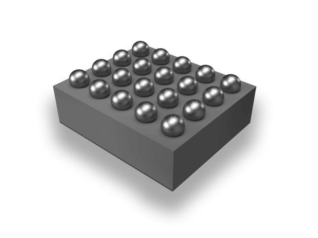
KTB8371 are available in RoHS and Green compliant 20-bump 1.7mm x 2.0mm x 0.6mm wafer-level chip-scale package (WLCSP20)


Features
- Wide VIN Range: 4.7V to 17V
- Maximum Continuous Output Current: 5A
- I2C Control Interface
- Programmable Output Voltage from 0.8V to 5.5V
- Integrated High / Low-Side FETs (65mΩ / 35mΩ)
- Advanced Adaptive On-Time Control
- Fast Transient Response
- ±0.5% Feedback Voltage Reference
- Zero Shutdown Supply Current
- 50μA Non-Switching Operating Quiescent Current
- 80μA No Load Operating Quiescent Current
- High Efficiency in Light Load and Heavy Load.
- Programmable Switching Frequency with 500kHz, 1MHz, 1.5MHz, and 2MHz options
- Internal Soft-Start
- Programmable Forced CCM, Automatic CCM/PFM
- Built-in Cycle-by-Cycle Current Limit, Short Circuit Protection, Input UVLO, Output Under-Voltage Protection, Output Over-Voltage Protection, and Thermal Shutdown Protection
- Small 20-bump WLCSP (1.7mm x 2.0mm)
Applications
- CPU, GPU, AP, DSP, FPGA, VIO, VSYS
- HDD, LPDDR3, LPDDR4 Memory Power
- Tablets, Netbooks, Ultra-Books, Mobile Internet Devices, IoT, and Server.
- DSC, Drones, Gaming Consoles, TV Set Box
| Package |
Dimensions |
Bumps |
Package Code |
| WLCSP45-20 |
1.750mm x 2.063mm x 0.620mm |
20 |
IB |
Parameters
| Vin (min) |
Vin (max) |
Switching Frequency (MHz) |
Max Current (A) |
| 4.7V |
17.0V |
Adj 0.5/1.0/1.5/2.0MHz |
5.0 |
Technical Documentation
Purchase
| Part Number |
Marking |
Operating Temperature |
Package |
| KTB8371AEIB-5C-TR |
OXXXYYZZZZ |
-40°C to +85°C |
WLCSP20 |
| KTB8371BEIB-5C-TR |
PBXXYYZZZZ |
-40°C to +85°C |
WLCSP20 |
| KTB8371CEIB-5C-TR |
PFXXYYZZZZ |
-40°C to +85°C |
WLCSP20 |


